
TechflierTechflierTechflier
  • Home
  • News
  • Features
  • Spotlight
  • About
    • Mission
    • Services
    • Contact
  • Newsletter
  • Shop
    • All Items
    • By Category
      • Bags
      • T-Shirts
    • Cart
Search
© 2025 Techflier. All Rights Reserved.
Reading: Huawei packs 4,000 AI chips into a single optical supernode
Share
Font ResizerAa
TechflierTechflier
Font ResizerAa
  • Home
  • News
  • Features
  • Spotlight
  • About
  • Newsletter
  • Shop
Search
  • Home
  • News
  • Features
  • Spotlight
  • About
    • Mission
    • Services
    • Contact
  • Newsletter
  • Shop
    • All Items
    • By Category
    • Cart
Have an existing account? Sign In
Follow US
© 2025 Techflier. All Rights Reserved.
News

Huawei packs 4,000 AI chips into a single optical supernode

Huawei's Ascend 960 SuperPoD links up to 4,096 NPUs through near-packaged optics, cutting power and module counts in very large AI clusters.

Techflier Staff
Last updated: September 18, 2026 1:15 am
Techflier
Share
SHARE

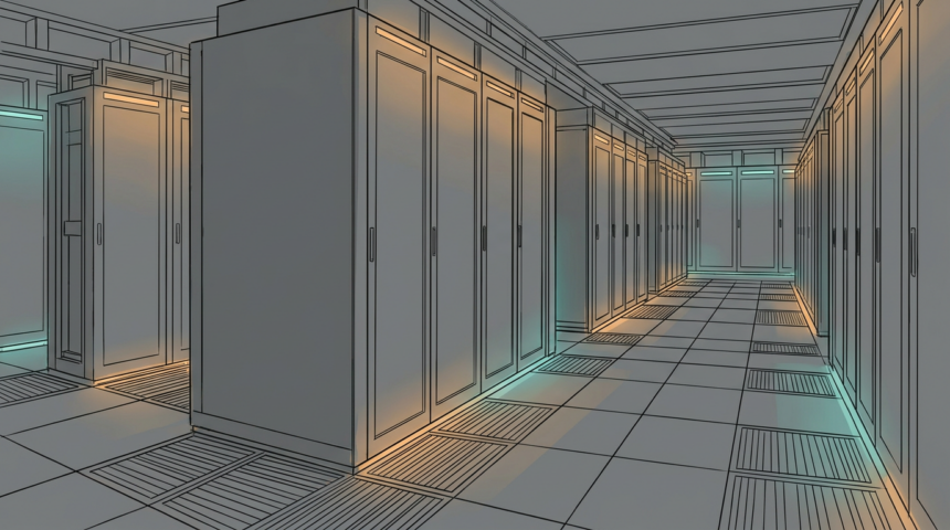
Huawei used its annual HUAWEI CONNECT keynote to unveil the Ascend 960 SuperPoD, which the company calls the industry’s first SuperPoD built on near-packaged optics.

The system links up to 4,096 NPU cards, delivering up to 8E FP8 compute and 1PB of HBM capacity. Huawei argues the architecture matters more than the headline numbers: in a 100,000-card cluster, chip-to-chip communication can eat more than 40% of training time under conventional server designs.

Its answer is NPO, or near-packaged optics, which moves optical components closer to the compute silicon so high-speed electrical signals travel shorter distances. Huawei’s Hi-ONE engine carries 7.2T of transmission capacity. Roughly 5,500 Hi-ONE units replace the 48,000 800G pluggable optical modules a comparable build would need, cutting power consumption by more than 550kW. Mean time between failures doubles, Huawei says, and availability reaches 99.8%.

Rotating chairman Wang Tao framed the launch around the agentic era, where models at the 10-trillion-parameter scale outgrow the wiring that connects them.

The pitch lands in a market where export controls have pushed Chinese labs toward domestic silicon. Huawei’s argument is that interconnect, memory and system design – not individual chips – decide who can train the largest models.


Jane Street bets on Etched chips as valuation doubles to $21B
Burger deliveries go airborne over Shanghai’s West Bund
Uber Freight alum raises $10M for portable nuclear reactors on floating barges
ESA hands Nyx capsule builder a €760M cargo contract
Portage leads €30M Moss round as fintech hits unicorn mark
TAGGED:AI ChipsAI infrastructureChina techdata centersHuaweisemiconductors
SOURCES:TechNode
Share This Article
Facebook Copy Link Print
Previous Article Tokyo’s CADDi hits $1.2B teaching AI to read factory blueprints
Next Article A $20B transatlantic merger tests Europe’s appetite for sovereign AI

Get Some Gear


Quick Links

  • News
  • Features
  • Spotlight
  • Newsletter
  • Store

About Techflier

  • About Techflier
  • Services
  • Contact Us
  • Privacy
  • Legal

Indices

TechflierTechflier
Follow US
© 2026 Techflier. All Rights Reserved.
Welcome Back!

Sign in to your account

Username or Email Address
Password

Lost your password?